Shenzhen Fanway Technology Co., Ltd.
PCB Assembly

PCB Assembly

Fanway specializes in delivering efficient and reliable end-to-end PCB assembly services, precisely tailored to your unique requirements to accelerate your product success.

High-Density PCB Circuit Board Assembly with BGA Package
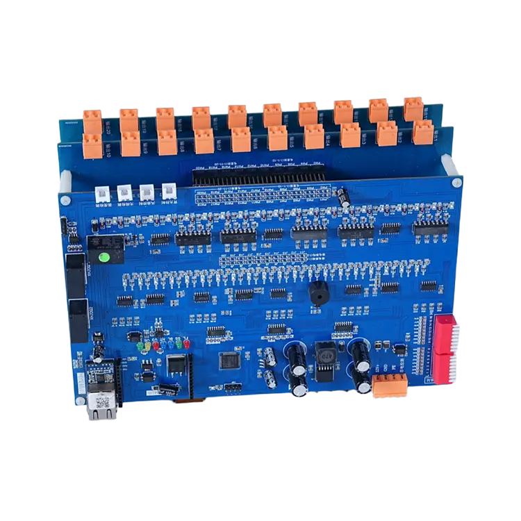
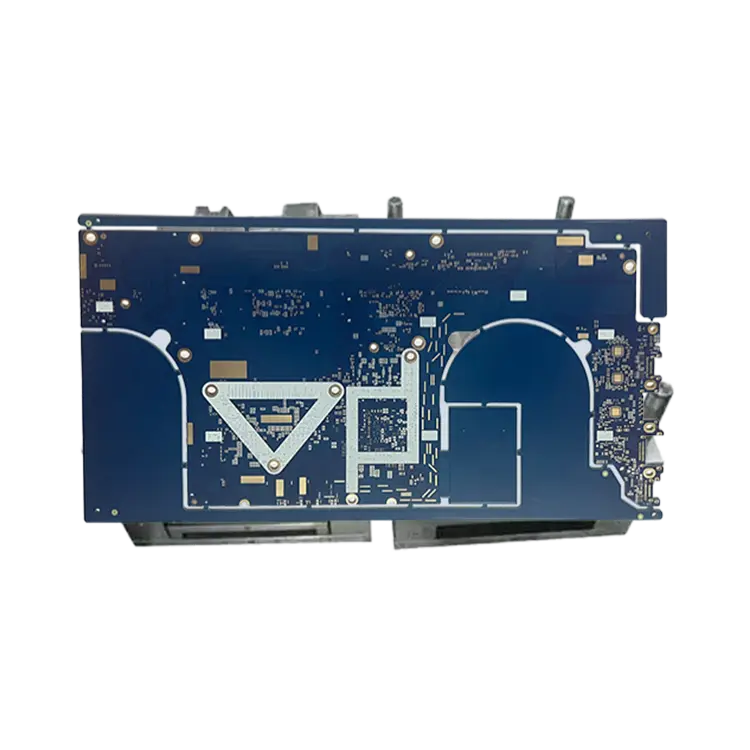
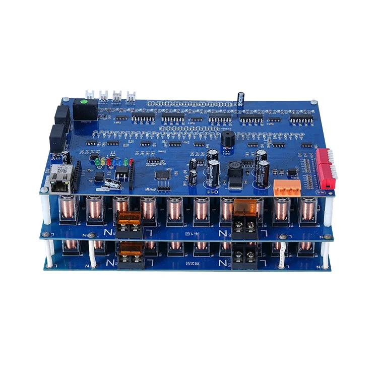
  • High-Density PCB Circuit Board Assembly with BGA PackageHigh-Density PCB Circuit Board Assembly with BGA Package

High-Density PCB Circuit Board Assembly with BGA Package

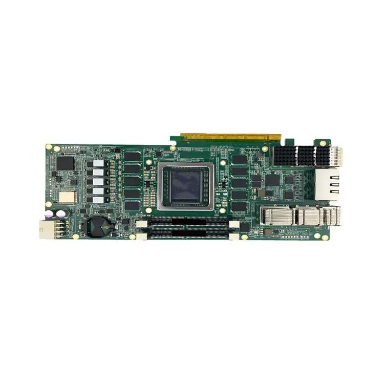
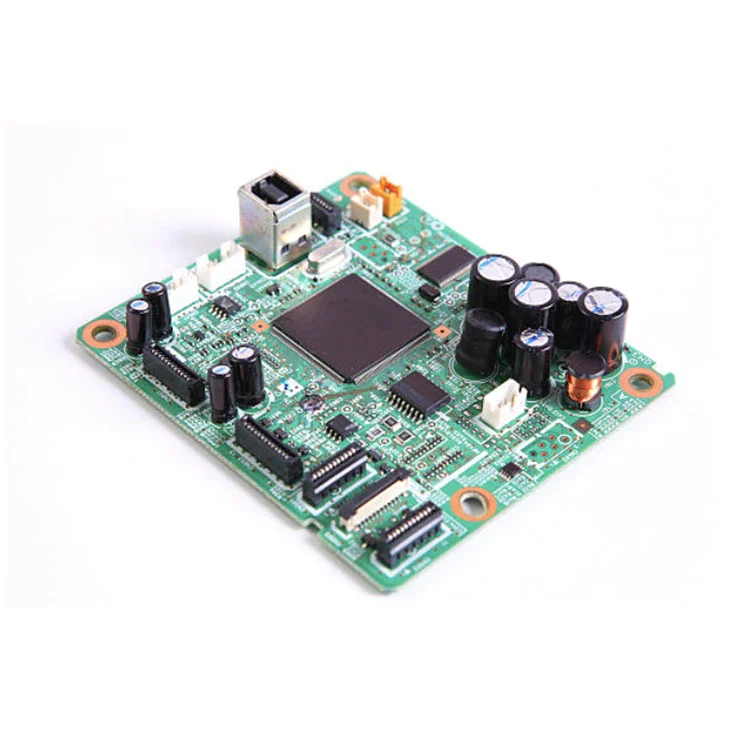
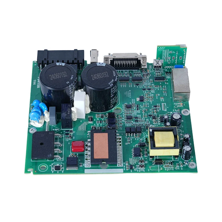
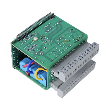
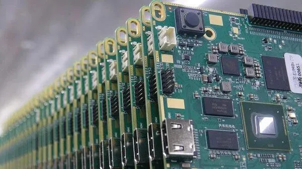
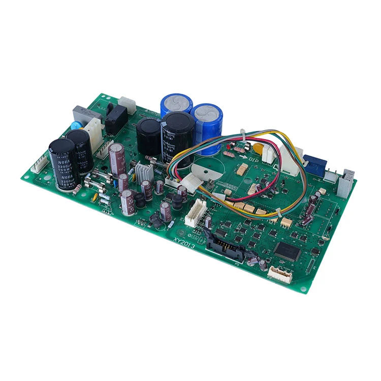
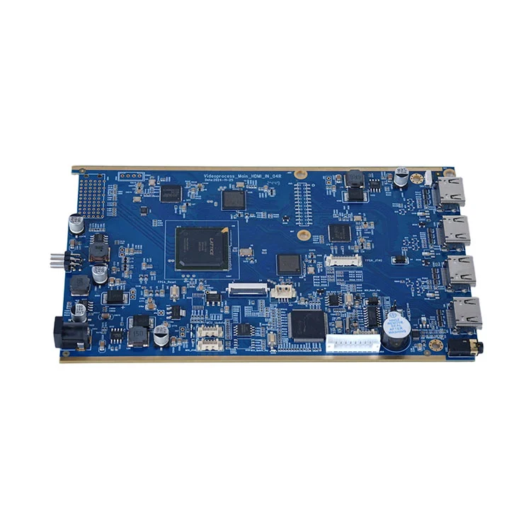
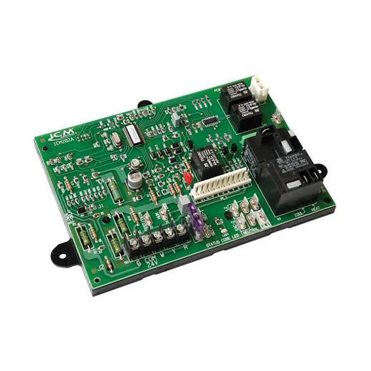
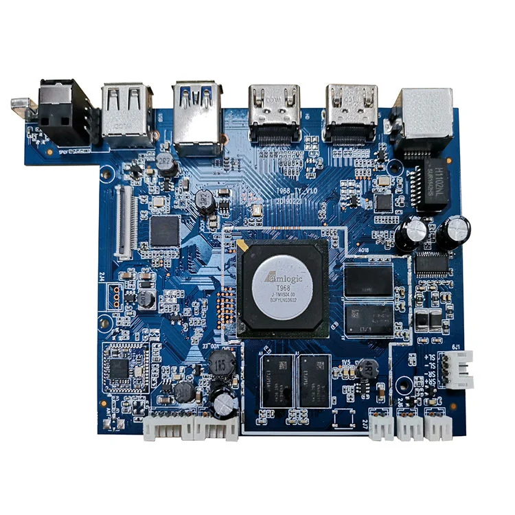
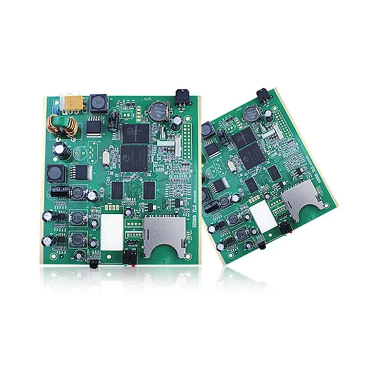
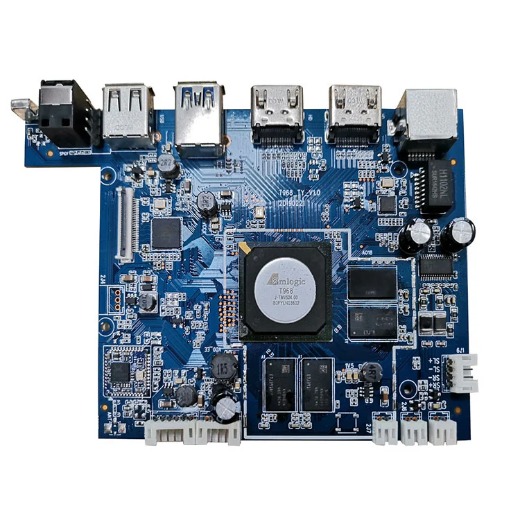
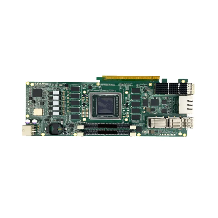
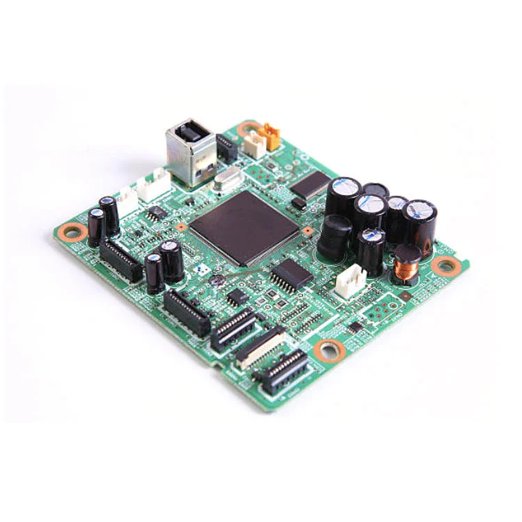
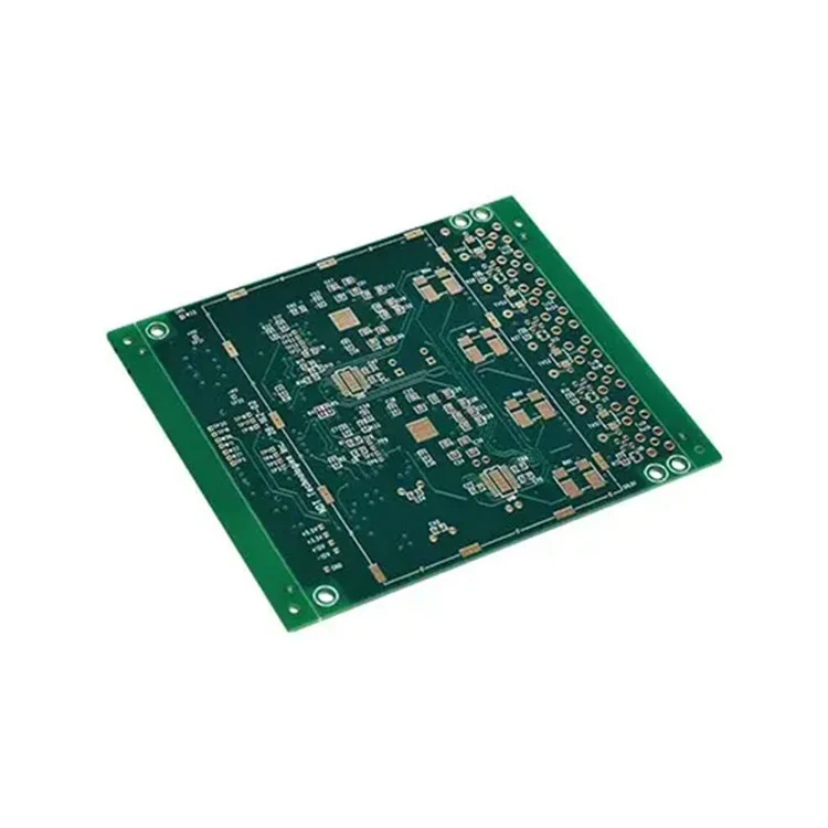
As a China PCB assembly manufacturer supplier, Fanway specializes in High-Density PCB Circuit Board Assembly with BGA Package services for hardware designs that require high I/O density and reliable interconnections in compact spaces with over 12 years of industry experience. BGA packaging supports hundreds of connections in a small footprint, with short paths that minimize signal loss. The BGA PCB Assembly covers prototype development through production, including component removal, rework, reballing, and X-ray inspection.

The High-Density PCB Circuit Board Assembly with BGA Package service from Fanway is suited for AI processors, telecommunications equipment, medical devices, and industrial controls. BGA packages are built with a silicon die for processing, an interconnect layer connecting the die to the substrate, and a solder ball array on the underside that attaches to the PCB. This design provides high connection density, short signal paths for better electrical performance, efficient heat transfer to the board, and a self-alignment feature during soldering that corrects minor placement offsets. Our service manages the full workflow from PCB layout support through assembly and final inspection.

Bga Pcb Assembly


How BGA Works?

BGA packages connect to the PCB through the solder ball array on the underside of the component. During the reflow process, all solder balls are heated simultaneously to melting point. The surface tension of the molten solder pulls the component into precise alignment with the PCB pads, forming electrical, mechanical, and thermal connections simultaneously. This self-alignment effect compensates for minor placement errors and is the reason BGA assemblies can achieve high yields despite the small pitch sizes.


What's the Advantages of BGA Packaging?

BGA packaging is the mainstream choice for high-end chips due to the following advantages.

High density 

It supports hundreds or thousands of connections in a compact footprint, enabling complex designs.

Superior electrical performance 

It comes from short interconnect paths that reduce inductance and resistance, effectively minimizing high-frequency signal distortion for RF and high-speed applications.

Better thermal management 

It occurs because solder balls conduct heat to the PCB more efficiently than traditional leads.

Self-alignment effect 

BGA Circuit Boards Surface Mount Assembly of PCB means that during reflow, the surface tension of molten solder automatically corrects minor placement deviations, improving assembly yield.


BGA Assembly Process

High-Density PCB Circuit Board Assembly with BGA Package is the most demanding segment of SMT assembly. Each step requires precise control to achieve reliable joints.

1. PCB Pad Design 

Two options exist. NSMD pads have no solder mask over the pad edges, providing consistent dimensions and stronger mechanical joints. SMD pads have solder mask covering the pad edges, concentrating thermal stress and resulting in smaller effective solder area. For high-speed digital circuits, NSMD is preferred. When BGA pitch decreases to 0.5mm or below, via-in-pad becomes necessary because traditional dog-bone fan-out cannot fit. Via filling and plating flatness are critical. Uneven surfaces create voids during reflow.

2. Stencil Design 

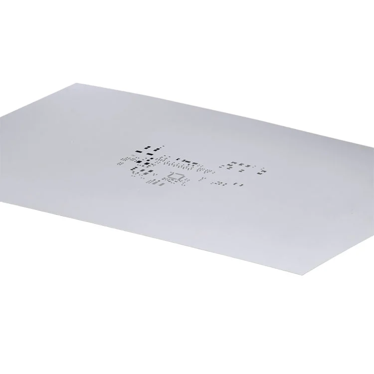
Stencil design determines solder paste volume. For fine-pitch BGA assemblies, laser-cut and electro-polished stencils with aperture size compensation are required. For 0.4mm pitch BGAs, stencil thickness is typically 0.1mm. Aperture size and shape are adjusted to achieve the correct paste volume for each BGA ball size.

3. Placement 

BGA components are placed using automated pick-and-place equipment with vision alignment. Placement accuracy of +/- 0.03mm ensures each solder ball aligns with its corresponding pad.

4. Reflow Soldering 

The reflow profile is the most critical parameter in BGA assembly. The profile consists of four stages. Preheat uses a 1 to 3°C per second ramp rate, reducing temperature differential between BGA and PCB to prevent warpage. Soak holds at 150 to 200°C for 60 to 90 seconds, activating flux and removing oxides. Reflow reaches peak temperature of 235 to 245°C for lead-free SAC305, with time above liquidus of 60 to 90 seconds. Cooling uses a 2 to 4°C per second cooling rate, refining grain structure for improved fatigue life. Temperatures below the minimum cause cold joints. Temperatures above the maximum damage the internal structure of the BGA component.


Fanway Technical Capabilities

The High-Density PCB Circuit Board Assembly with BGA Package service from Fanway includes the following technical capabilities.

BGA Size Range: Assembling BGA components from 1x1mm to 50x50mm, covering micro BGAs for portable devices and large body FCBGAs for high-performance processors.

Pitch Size: Minimum pitch of 0.4mm with placement accuracy of +/- 0.03mm. Pitches below 0.4mm are evaluated case by case.

Board Layer Count: Assembly support for boards from 1 to 108 layers, covering simple double-sided boards through complex high-layer-count backplanes.

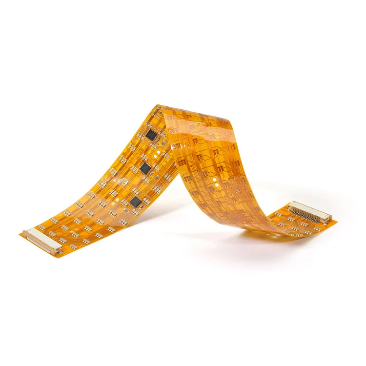
Board Thickness: Supports board thickness from 0.2mm to 10.0mm, covering flex circuits through rigid backplanes.

Passive Component Support: Assembles passive components down to 01005 and 0201 alongside BGA packages on the same board.

Solder Balls: Supports both leaded and lead-free solder alloys.

Certifications: ISO9001, ISO14001, ISO13485, RoHS, IPC.


Applications

BGA PCB assembly is essential for applications requiring high I/O density, signal integrity, and thermal performance. The High-Density PCB Circuit Board Assembly with BGA Package serves these key sectors.

AI and High-Performance Computing: GPUs, AI accelerators, and server processors use large FCBGA packages with thousands of connections.

Telecommunications: 5G baseband chips, network processors, and switching ASICs require fine-pitch BGA for high-speed data transmission.

Medical Devices: Diagnostic imaging equipment, patient monitors, and portable medical instruments use BGA for compact, reliable electronics.

Industrial Control: PLCs, motor drives, and automation controllers use BGA for processing and communication functions.

Consumer Electronics: Smartphones, tablets, and wearables use micro BGA for space-constrained designs.


Why Work with Fanway for your BGA PCB Assembly?

Precision Placement Equipment 

Placement accuracy of +/- 0.03mm supports fine-pitch BGA down to 0.4mm.

Controlled Reflow Profiling 

Multi-zone reflow ovens enable precise thermal profiles for different BGA package types and solder alloys.

X-ray Inspection 

2D and 3D X-ray systems verify joint quality for every BGA on every board.

BGA Rework and Reballing 

Dedicated rework stations with controlled thermal profiles perform BGA removal, pad cleaning, reballing, and replacement to IPC-7711/7721 standards.

Design Support 

PCB layout consultation for BGA routing optimization, including pad design recommendations and via-in-pad strategies.

Complete Service 

From PCB layout optimization through component sourcing, assembly, inspection, and rework, all through a single point of contact.

Certifications 

ISO9001, ISO14001, ISO13485, RoHS, IPC, with assembly processes compliant to IPC-A-610 and IPC-7095 standards.


Customized BGA Assembly Services

Fanway provides customized High-Density PCB Circuit Board Assembly with BGA Package services tailored to specific design and production requirements.

Design Support Our engineering team works with you during the PCB layout phase to optimize pad design, via placement, and fan-out routing for BGA packages, reducing the risk of assembly issues before production begins.

Component Sourcing We handle procurement of BGA components through authorised supply chains, ensuring authenticity and traceability. For components with long lead times or end-of-life status, we provide alternative recommendations.

Assembly Options Services include prototype assembly, volume production, rework, reballing, and component replacement. We adapt to your project stage and schedule requirements.

Customised Testing Test protocols are defined per project, not applied uniformly. We tailor inspection and testing to the specific BGA package type, board complexity, and application requirements.

Packaging and Delivery Boards are cleaned, coated if specified, packaged per ESD standards, and shipped with full traceability documentation to your designated location.


FAQ

Q: What is the minimum BGA pitch Fanway can assemble?
A: Fanway supports BGA assembly down to 0.4mm pitch as standard. Pitches below 0.4mm are evaluated case by case.

Q: Does Fanway provide design support for BGA assembly?
A: Yes. Fanway provides PCB layout consultation for BGA routing optimization, including recommendations on pad design, via-in-pad filling, and fan-out strategies.

Q: What is the typical turnaround time for BGA assembly?
A: Prototype BGA assemblies typically ship within 5 to 7 working days. Volume orders are scheduled based on component availability and board complexity. Expedited services are available.

Q: Can Fanway rework a BGA that has failed?
A: Yes. Fanway provides BGA removal, pad cleaning, reballing, and replacement using dedicated rework stations with controlled thermal profiles. Rework is performed to IPC-7711/7721 standards.

Q: What BGA package types does Fanway support?
A: Fanway supports PBGA, CBGA, FCBGA, Micro BGA, and LGA packages, as well as µBGA, CTBGA, CABGA, CVBGA, and VFBGA.

Hot Tags: High-Density PCB Circuit Board Assembly with BGA Package
Send Inquiry
Contact Info
  • Address

    Building 3, The First Industrial Zone of Mingjinhai, Shiyan Street, Bao'an District, Shenzhen, Guangdong, China, Zip Code:518108

For inquiries about printed circuit board, electronics manufacturing, pcb assembly please leave your email to us and we will be in touch within 24 hours.
X
We use cookies to offer you a better browsing experience, analyze site traffic and personalize content. By using this site, you agree to our use of cookies.Privacy Policy
RejectAccept