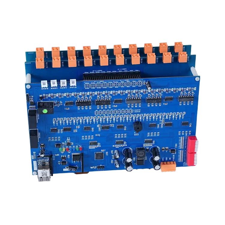
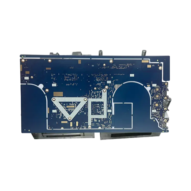
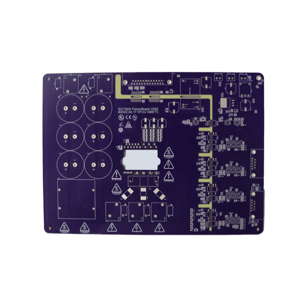
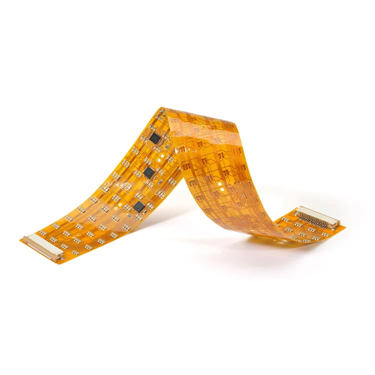
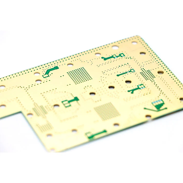
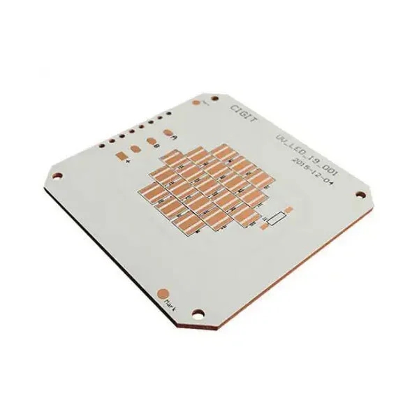
The relentless push toward smaller, faster, and more powerful electronic devices has driven significant innovation in printed circuit board technology. High-Density Interconnect (HDI) PCBs have become the foundation for today's most advanced electronics—from smartphones and wearables to automotive safety systems and medical implants. We examine what makes HDI PCBs different from conventional boards, the key technologies involved, and how Fanway's manufacturing capabilities support the production of these complex, high-reliability boards. We explore the design considerations, material choices, and quality standards that define modern HDI fabrication.
The Evolution of PCB Technology
The printed circuit board is the foundation of nearly every electronic device. As devices have become more powerful and more compact, the demands placed on PCBs have increased dramatically. Standard PCBs with through-hole components and wider traces are no longer sufficient for many modern applications. The need for higher component density, faster signal speeds, and reduced form factors has driven the adoption of High-Density Interconnect technology.
HDI PCBs achieve greater wiring density per unit area through a combination of finer lines and spaces, smaller vias, and higher connection pad densities. These boards enable the integration of more functionality into smaller spaces—a requirement for applications ranging from 5G communications infrastructure to medical diagnostic equipment and advanced driver assistance systems in vehicles.
Fanway Technology is a China-based Electronic Manufacturing Service provider with over 12 years of experience in PCB fabrication, assembly, and testing. The company offers end-to-end solutions from PCB layout and design to finished product delivery. This article provides an objective look at HDI PCB technology, the manufacturing processes involved, and the capabilities that make Fanway a partner for clients requiring high-density interconnect solutions.
What Makes HDI PCB Different?
HDI PCBs are distinguished from conventional PCBs by several key features that enable higher component density and better electrical performance.
Finer Trace Widths and Spaces
HDI boards can achieve trace widths and spaces as small as 2.5 mil (0.0635 mm) or even less. This allows more routing in a given area, making it possible to connect high-pin-count components like BGAs (Ball Grid Arrays) without requiring multiple layers or oversized boards.
Microvias
Unlike traditional through-hole vias that pass through the entire board thickness, microvias are small-diameter vias—typically less than 150μm—that connect adjacent layers. The smaller size allows for more vias in a given area and reduces the space consumed by the via itself.
Blind and Buried Vias
Blind vias connect an outer layer to an inner layer without penetrating the entire board. Buried vias connect inner layers without reaching the outer surfaces. These via types allow for more complex interconnections without consuming space on outer layers.
Thinner Dielectric Materials
The insulating layers between copper layers are thinner in HDI boards, contributing to reduced overall board thickness and improved signal integrity through shorter signal paths.
These features collectively enable significant board size reduction—sometimes up to 60% compared to conventional designs—while maintaining or improving electrical performance.
HDI PCB Classification and Complexity Levels
Not all HDI boards are equal. The complexity of an HDI design is typically categorized by the number of build-up layers and the via structures involved.
The "N" in the structure notation represents the number of core layers. Higher complexity boards require more sophisticated manufacturing processes and tighter process control.
Fanway has developed manufacturing capabilities to support a wide range of HDI PCB requirements. The following table summarizes the key capabilities available.
Capability
Range
Layer Count
1 – 108 layers
Finished Board Thickness
0.2 mm – 10.0 mm
Maximum Panel Size
610 mm × 1200 mm
Finished Copper Thickness
0.5 oz – 12 oz
Minimum Line Width / Space
2.5 mil / 2.5 mil
Minimum Finished Hole Size
0.1 mm
Maximum Aspect Ratio
25:1
Impedance Control Tolerance
±10%
The company also offers a range of surface finishes including HASL (LF), ENIG (Immersion Gold), Immersion Tin, Immersion Silver, OSP, and gold fingers, allowing customers to select the appropriate finish for their specific application and environmental requirements.
Quality and Certification Standards
HDI PCBs are typically used in applications where reliability is critical. Fanway maintains several quality certifications that reflect its commitment to meeting international standards.
• ISO 9001:2015 – Quality management system certification.
• IATF 16949:2016 – Automotive industry quality management standard.
• ISO 13485:2016 – Medical device quality management system certification.
The company also adheres to IPC standards, including IPC-A-600G for acceptability of printed boards and IPC-6012 for performance specification of rigid PCBs. HDI PCB production is available to IPC Class 2 and Class 3 standards, with Class 3 representing the highest level for mission-critical applications.
Environmental compliance includes UL safety certification, RoHS compliance for hazardous substance restriction, and REACH chemical compliance.
Frequently Asked Questions
Q: What is the difference between a standard PCB and an HDI PCB?
A: HDI PCBs feature finer trace widths (down to 2.5 mil), smaller vias (microvias under 150μm), and higher connection pad density. They enable more compact designs with better signal integrity compared to standard PCBs.
Q: What are microvias and why are they important?
A: Microvias are small-diameter vias, typically less than 150μm, that connect adjacent layers. Their smaller size allows for higher routing density and reduces the space consumed by the via structure.
Q: What is the maximum layer count Fanway can produce for HDI PCBs?
A: Fanway can produce HDI PCBs with up to 108 layers, depending on the design requirements and material selection.
Q: What certifications does Fanway hold for HDI PCB production?
A: Fanway holds ISO 9001:2015, IATF 16949:2016, and ISO 13485:2016 certifications. The company also adheres to IPC standards and maintains UL, RoHS, and REACH compliance.
Q: What surface finishes are available for HDI PCBs?
A: Available finishes include HASL (LF), ENIG (Immersion Gold), Immersion Tin, Immersion Silver, OSP, and gold fingers. The choice depends on the application's soldering requirements and environmental conditions.
Conclusion
HDI PCB technology has become essential for modern electronic devices that require higher functionality in smaller form factors. The combination of finer traces, microvias, and advanced materials enables designs that would not be possible with conventional PCB technology.
Fanwayoffers a comprehensive set of HDI PCB manufacturing capabilities, with layer counts up to 108, minimum trace widths of 2.5 mil, and support for a range of high-frequency and high-speed materials. The company's quality certifications—including ISO 9001, IATF 16949, and ISO 13485—reflect its commitment to meeting the requirements of automotive, medical, and other demanding applications.
With rapid prototyping options and free DFM analysis, Fanway provides practical support for customers developing new HDI designs. If you are looking for a reliable partner for your project, we invite you to contact Fanway today. The technical team can provide design guidance, material recommendations, and competitive pricing tailored to your specific requirements. Reach out through the company website or email to start the conversation.
We use cookies to offer you a better browsing experience, analyze site traffic and personalize content. By using this site, you agree to our use of cookies.Privacy Policy